
The semiconductor industry demands extremely high levels of precision and cleanliness during manufacturing. Even microscopic particles or environmental contaminants can compromise the functionality of semiconductor devices, resulting in defects, reduced yields, or product failure. To address these challenges, manufacturers rely on ISO Class 5 cleanrooms, which provide controlled environments with strict limits on airborne particle concentrations and environmental variables. These cleanrooms are essential for ensuring the quality, reliability, and performance of semiconductor components.
ISO Class 5 cleanrooms are defined by the ISO 14644-1 standard, which allows no more than 3,520 particles of 0.5 micrometers or larger per cubic meter. This high level of cleanliness is achieved through advanced filtration systems, laminar airflow design, environmental monitoring, and strict operational protocols. For organizations exploring the implementation of such facilities, resources such as the ISO Class 5 Cleanroom provide comprehensive guidance on classification standards, design principles, and operational best practices tailored to high-precision industries like semiconductors.
Role of ISO Class 5 Cleanrooms in Semiconductor Manufacturing
Semiconductor manufacturing involves complex processes, including photolithography, chemical vapor deposition, etching, doping, and wafer handling. These processes are extremely sensitive to airborne contaminants, moisture, and particulate matter. An ISO Class 5 cleanroom provides a controlled environment that minimizes the presence of these contaminants, ensuring process reliability and high product yield.
In photolithography, for example, even a single particle landing on a silicon wafer can disrupt the delicate patterns used to create integrated circuits. Laminar airflow and HEPA or ULPA filtration in ISO Class 5 cleanrooms help maintain particle-free conditions on wafer surfaces, preventing defects and improving overall production efficiency. Similarly, chemical processes require precise temperature and humidity control to ensure consistency and avoid unwanted reactions, which is supported by the environmental stability of ISO Class 5 cleanrooms.
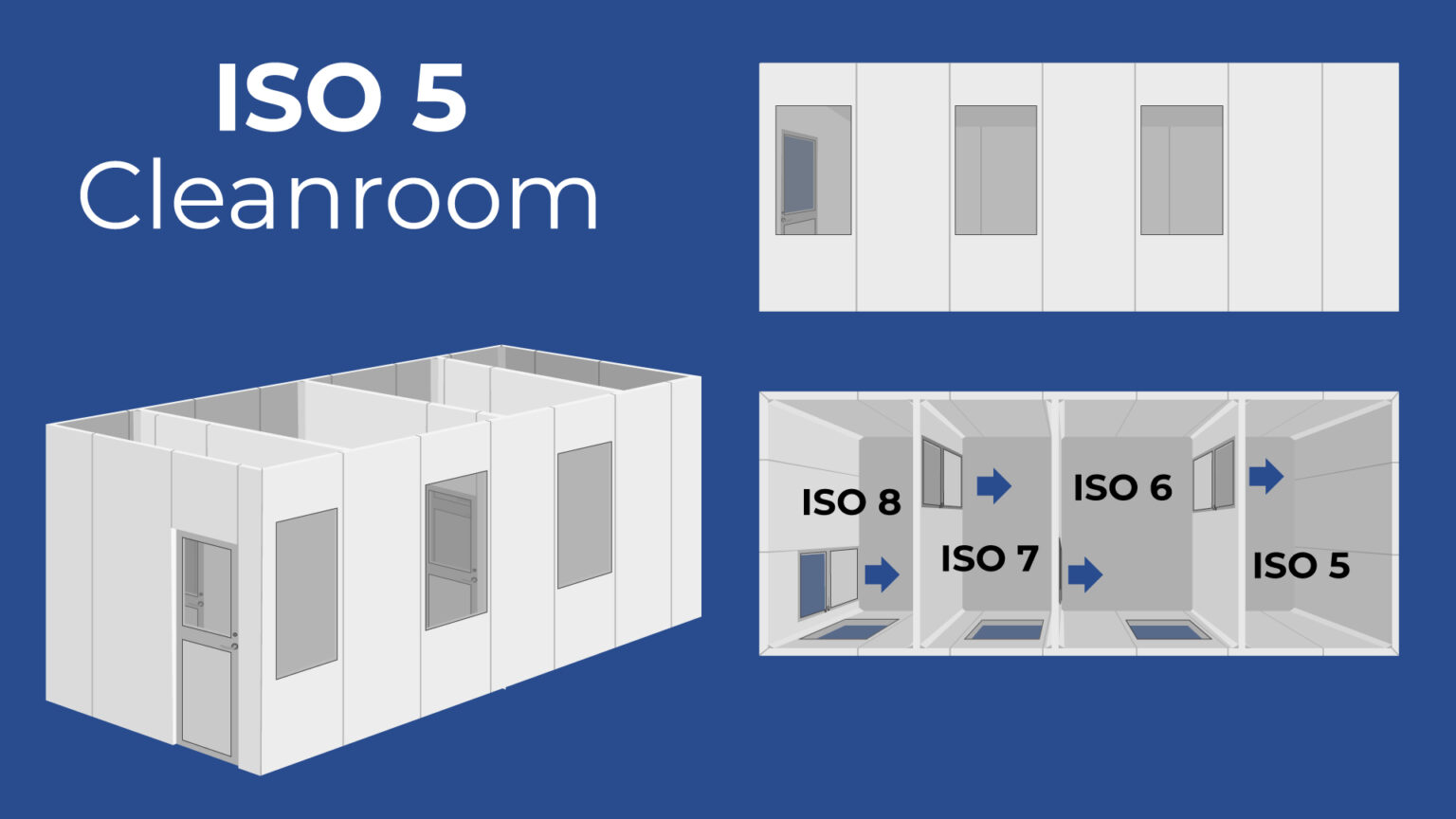
Cleanroom Design Considerations for Semiconductor Applications
The design of ISO Class 5 cleanrooms for semiconductor applications emphasizes airflow management, filtration, and material flow. Unidirectional or laminar airflow is critical for sweeping airborne particles away from sensitive areas. Ceiling-mounted HEPA or ULPA filters provide continuous removal of contaminants, while carefully designed air change rates ensure consistent particle control throughout the cleanroom.
Equipment placement is another key consideration. Tools, benches, and robotic systems are positioned to maintain unobstructed airflow and reduce turbulence that could lead to particle accumulation. Additionally, workstations are designed for easy cleaning and maintenance, which is essential to sustain ISO Class 5 standards over time. Modular designs and flexible layouts also enable manufacturers to adapt to evolving process requirements without compromising cleanliness.
Environmental Control and Monitoring
ISO Class 5 cleanrooms in semiconductor manufacturing require precise control over temperature, humidity, and pressure differentials. Maintaining stable environmental conditions is essential because small fluctuations can affect wafer processing, chemical deposition, and etching uniformity. Humidity control is particularly important to prevent electrostatic discharge, which can damage sensitive semiconductor devices.
Continuous monitoring systems track airborne particles, airflow velocity, pressure, temperature, and humidity in real time. Any deviation from established thresholds triggers alerts and corrective actions. Regular validation and testing of these parameters are conducted to ensure compliance with ISO standards and to maintain a contamination-free manufacturing environment.
Personnel and Operational Protocols
Human activity is a major source of contamination in semiconductor cleanrooms. ISO Class 5 cleanrooms enforce strict gowning and behavior protocols to minimize particulate generation. Personnel are required to wear full cleanroom suits, gloves, masks, and shoe covers made from non-shedding materials. Entry and exit procedures involve gowning rooms and airlocks to maintain positive pressure and prevent particle ingress.
Operational protocols also include restricted access to sensitive areas, proper handling of materials, and regular cleaning of work surfaces and equipment. Automated systems, such as robotic wafer transport and material handling, further reduce human interaction with critical processes, lowering the risk of contamination and enhancing process consistency.
Applications in Semiconductor Processes
ISO Class 5 cleanrooms support several critical semiconductor processes. These include:
- Wafer Fabrication: Controlling particle levels during lithography, etching, and deposition ensures high yield and precision.
- Packaging and Assembly: Protecting delicate chips from particulate contamination during assembly and wire bonding is essential for device reliability.
- Testing and Inspection: Particle-free environments prevent errors in automated optical inspection systems and functional testing stations.
- Advanced Chip Production: Cutting-edge semiconductor nodes with extremely fine features require ultra-clean environments to prevent even submicron particles from causing defects.
Advantages of ISO Class 5 Cleanrooms in Semiconductor Industries
Using ISO Class 5 cleanrooms allows semiconductor manufacturers to improve yield, reduce product defects, and maintain consistency across production batches. Controlled environments also enable the adoption of advanced technologies, such as extreme ultraviolet (EUV) lithography, which demands stringent contamination control. Additionally, adherence to ISO standards ensures regulatory compliance and enhances the company’s reputation for quality and reliability.
Conclusion
ISO Class 5 cleanrooms are indispensable in the semiconductor industry, providing a controlled environment necessary for high-precision manufacturing processes. From wafer fabrication to packaging and testing, these cleanrooms minimize contamination risks, maintain environmental stability, and support advanced semiconductor technologies. By implementing rigorous design, operational, and monitoring practices, semiconductor manufacturers can achieve higher yields, lower defect rates, and consistent product performance, ensuring success in a highly competitive and technologically demanding industry.